Web Page Introduction
Basic Resistance-Capacitance Filter Design
The normal response of these networks is a 6dB drop in output voltage per octave. A faster drop can be achieved by cascading filters in series as is shown in Figure 1 with the series lowpass filter using 2 networks. Unfortunately, interactions between the two series filter sections will change the cutoff frequency from the design frequency somewhat. Lowpass, highpass, bandpass and band-reject (notch) filters can be made using RC networks although this web page will focus mainly on the lowpass and bandpass types.
Although, many amateurs are now using LC network designs or low-noise operational amps for receiver audio filters, RC filters using discrete components can be low cost and practical alternatives. RC networks enjoy some advantage over LC networks, namely they do not pickup inductive hum and they are frequently less expensive and more compact in size.

Interstage Filters
Discussion
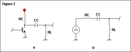
Every amplifier has an optimal frequency range that it will operate over. RC-coupled stages maybe designed to operate over a frequency range that best suits the radio amateur. In Figure 2a , we see can see that the coupling capacitor CC is really in series with the two resistors RC and RL. At midrange to high audio frequencies, the reactance of CC is negligible and there will be very little AC voltage drop over it. If we lower the audio frequency, the capacitive reactance CC will increase by the formula XC = 1 / 6.283 x Frequency x CC. The lower the frequency, the greater the voltage drop across capacitor CC will be. If the frequency is lowered to the point where the the capacitive reactance of CC is equal to the the series resistance of the circuit the AC voltage drop will be 3dB down from the source voltage.
Figure 2b shows the voltage source equivalent of figure 2a. In these diagrams, it is important to note that the value of RL represents the total input impedance of the subsequent transistor stage. For a given RC and RL, the greater the CC value, the greater the low frequency response. This fact is often conversely used by radio amateurs to attenuate 60 cycle hum by using high value capacitors such as 0.1uF for coupling caps.
Emitter bypass caps also can have an effect on the low frequency response of an amplifier. The lower the XC of an emitter bypass cap, the greater the low frequency response. A rule of thumb is to use a bypass capacitor with an XC of 100 or less at the lowest frequency you wish to amplify.
Project
The basic design formulas are shown however they do require some clarification.
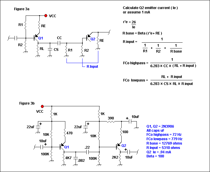
The 3dB highpass cutoff frequency is the frequency where the reactance of of the coupling capacitor CC equals the series resistance of the input impedance of Q2 plus resistor RL of Q1. While the RL value is straight forward, the input impedance is a more complex affair. Figure 2a shows how Q2 looks in terms of its AC input resistance. The input resistance is composed of R1, R2 and the Q2 emitter resistor. In order to calculate the AC emitter resistance, the DC emitter Current (Ie) must be first calculated using a calculator or computer program. Get a transistor textbook if you do not know how to do this or just assume 1 mA for Ie. To calculate the AC emitter resistance r'e in ohms, divide Ie into 26.
The formulas are shown in Figure 3a. The base resistance is calculated by multiplying the transistor Beta by the sum of r'e plus RE which is the resistance value of the component resistors hooked to the Q2 emitter. If the emitter is bypassed, make RE zero, if emitter degeneration is used, the resistance value RE will be the resistance of the unbypassed resistor. To solve for the AC input resistance, use the parallel circuit formula for R1, R2 and R input.
The 3dB lowpass cutoff frequency is is the frequency in which the reactance of the shunt capacitor CS is equal to the resistance of RL in parallel with the input resistance of Q2 (R input calculated as above).
Figure 3b shows a practical interstage filter with a low and highpass cutoff near the desired 10 times differential. Of interest, is the emitter degeneration on Q2. This is done to raise the AC input resistance of Q2, stabalize the amp, reduce distortion and to aid in setting the filter capacitor values. The calculated values are shown to the right of the figure 3b schematic.
A PSPICE run of the 3b interstage filter can be found on this AF Filter Supplemental Page
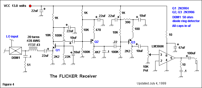
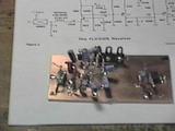
The Flicker Receiver
The 3 stage preamplifiers have
considerable gain and drive the final and headphones with good volume. At full
volume, AF feedback may erupt if leads and connecting wires are excessively
long. Although my version does not have hum problems, one possible improvement
would be to add the active decoupler to the first stage. It is found in every
other receiver on this web site and would minimize any chance of 60 Hertz hum
getting into the Q1 stage. This little receiver does a good job for so few parts
and can be built extremely compactly.
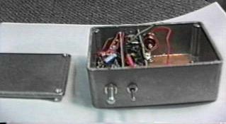
Below the prototype board is an actual receiver with an antenna
lowpass filter installed in a Hammond 4 X 3 inch die-cast case as part of a
personal version of W7ZOI's MicroMountaineer transceiver. The loose red and
black wires are temporary B+ and antenna cables used in testing the receiver.
The crystal oscillator, sidetone and transmitter stages have not yet been
installed. The transmitter puts out 1 watt onto the 30 Meter band and features
solid state T/R switching. This is one of my all time favorite projects and has
provided many hours of fun and even some DX.
I have built a few successful
active filters using nJFETs in both common drain and as source followers. With
these transistors, the low frequency calculations are similar to those of BJTs.
To use the Figure 3a formula for the highpass 3dB cutoff frequency, R input
would be the gate resistance and RL the source resistance of the previous stage.
For the high frequency calculations, things get more complex and the effects of
the circuit and component capacitance come into play. The lowpass formula maybe
used but the CS value will be a bit low in most cases. The actual 3dB cutoff
value maybe somewhat different than the design value. Experimentation will lead
you to good fun and enhanced knowledge of electronics.
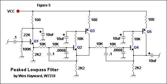
Fourth Order Peaked Lowpass Audio Filter
Peaked Lowpass Filter
The Q of each filter pair is 1.9
giving a 6dB bandwidth of 200 Hertz. The center frequency is 540 Hertz and
attenuation of the ten pole filter is 75dB at 1200 Hertz. The net gain of the
ten pole filter is 28 dB. Transistor choices include 2N3904 or lower noise
equivalents for the NPN transistors and 2N3906 or lower noise equivalents for
the PNP BJTs. example: 2N3565, 2N5089, 2N5087, 2N3638 etc. Allowable component
tolerances are 10 - 20 % with minimal degradation of performance.
A PSPICE
run of the 4 pole filter shown can be found on this AF Filter Supplemental
Page
Solid State Design for the Radio Amateur contains additional
useful information on building discrete component audio filters. For fun, I
connected the 4 pole filter to a modified Flicker receiver prototype and was
suitably impressed.
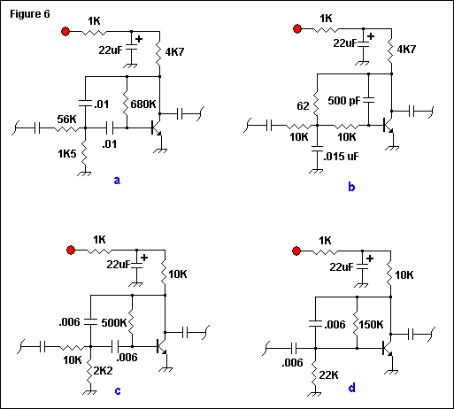
Miscellaneous Filters
Single
common emitter audio filter/amplifier stages maybe used in popcorn receivers.
Below is a collection of four such amplifiers. Figure A has a 300 hertz
bandwidth with a center frequency of 800 hertz. Voltage gain is 1. Figure B has
a low pass response with a breakaway frequency of 3 KHz. Figure C has a bandpass
response center frequency of 1 KHz and is Figures B and D cascaded. Figure D has
a highpass response with a cutoff frequency of 360 Hz. Figure B, B and D have a
no load voltage gain of ~20. All filters can be built using the ubiquitous
2N3904 or equivalent NPN BJT. The cutoff frequencies maybe changed up tp three
decades by changing the capacitor values by a common factor. Trial and error or
SPICE simulation are practical approaches as no design equations are available.