|
|
|
|
|
|
|
|
by Adam Farson, VA7OJ/AB4OJ, May 2002
Introduction: A solid-state HF amplifier differs fundamentally in its design concept from a tube amplifier. Vacuum tubes operate at high anode voltages and moderate anode currents; typically, a tube PA (power amplifier) stage requires an RF anode load resistance of approximately 2000Ω for optimum efficiency. Modern tube amplifiers are single-ended, with one or more tubes. Multiple devices are connected in parallel; a tuned output tank circuit, such as a pi (or pi-L) network, is used to transform the load resistance to the nominal 50Ω load. A working Q of 12 ensures adequate harmonic suppression.
The RF input circuit of a vacuum-tube amplifier may be either broadband or broadly-tuned. Grounded-grid configurations are most often encountered in modern tube amplifier designs.
The topology of a solid-state PA stage is quite different. The relatively low voltages and high currents required by the RF power transistors (typically 50V at 40A for a 1 kW amplifier) dictate a low collector (or drain) load resistance, of the order of 3Ω for a 250W PA module. The difficulty of matching the low impedances involved here to a 50Ω resistive load over a wide frequency range has dictated a broadband, base-driven (or gate-driven) architecture, using ferrite-cored input and output matching transformers. A working Q of unity or less is not uncommon; these matching networks thus offer no harmonic suppression.
The output-transformer secondary expects to see a 50Ω resistive load. The input-transformer primary presents a 50Ω resistive load to the source over its entire frequency range; thus, tuned input networks are not required. The exciter always sees 50Ω resistive. It is therefore unnecessary to engage the transceivers auto-tuner when driving a solid-state amplifier.
The RF matching transformers used in solid-state PA stages are wound on rectangular "binocular" 2-hole ferrite cores. Bifilar or trifilar windings made with miniature coaxial cable are used. These are designed in such a way that the series reactance and resistance of the windings is very small compared to the already very low RF load resistance, or input resistance, of the power devices. Ferrite cores must always be sufficiently large to avoid saturation at full RF drive or output. Such saturation is a major cause of intermodulation distortion. The transformer cores are thermally coupled to the heat dissipator, and/or mounted in the cooling-air stream, to remove heat caused by iron loss. (Reference 3)
The PA stage is always push-pull; this minimises even-harmonic generation. A matched pair of RF power devices is always used. Typically, a PA module (one pair of devices) is designed for 250W RF output; two modules are combined for 500W, and four for 1 kW. Each module is, in fact, a larger version of the PA stage found in popular 100W-class HF transceivers.
In a 500W-class amplifier, a 3-port hybrid-transformer power-splitter divides the drive power equally between two 250W modules. A 3-port hybrid power-combiner adds the two module outputs to produce 500W. A 1 kW-class amplifier is made up of four 250W PA modules; the splitter and combiner are 5-port circuits. The transformer construction in the splitter and combiner is as described above.
Why 3 and 5 ports? The splitter has 1 input and 2 or 4 outputs. Conversely, the combiner has 2 or 4 inputs and 1 output.
The combiner output is fed to a bank of bandswitched low-pass filters (LPF). These filters are designed to suppress harmonics and spurious emissions to levels required by radio regulations (typically 46 dBc or lower). The output of the filter bank is routed via the output T/R relay to a reflectometer, and thence via the internal auto-tuner (if fitted) to the antenna connector.
The splitter and combiner ports must be correctly terminated in 50Ω resistive. A mismatch can cause saturation of the transformer cores, leading to IMD degradation, and can also produce excessive dissipation in the hybrid balancing resistors.
The input connector is wired via the input T/R relay to the input port of the splitter.
So there we have it the basic, broadband, no-tune (or self-tuning) solid-state HF amplifier.
Now, we can ask: What makes a good solid-state HF amp?
The building-blocks of a typical solid-state amplifier are as follows:
1. PA stage. Let us start here, at the heart of the amplifier. These are the qualities to look for:
Adequate cooling and duty cycle: The efficiency of a solid-state Class AB amplifier typically runs around 45 ~ 50%. Thus, the PA stage should incorporate a heatsink or heat-dissipator system capable of dissipating at least half the DC input power, whilst maintaining a safe transistor case temperature.
Typically, the PA cooling system should be designed to keep the device case temperature in the range 70 ~ 80ºC (158 ~ 176ºF) at 25ºC (77ºF) ambient, for a 30-minute SSB voice transmission or a 5- to 10-minute key-down CW transmission at rated output. These are minimal duty cycle values for an amplifier operating in average amateur service. Longer key-down intervals, necessitating larger heat-dissipating surfaces and greater air circulation, are required for contest operation or at high ambient temperatures. Some amplifier manufacturers specify the power-output rating as ICAS (Intermittent Commercial and Amateur Service).
The physical configuration of the amplifiers cooling system can be either a large, finned planar heatsink with fans blowing air across it, a cylindrical heatsink structure through which a fan moves a large volume of air, or a thermodynamic heat-exchanger. The latter is an innovative approach, in which the power devices are mounted on hollow blocks through which a refrigerant circulates. The evaporation of the refrigerant cools the devices, and the vapour is re-condensed by blowing cooling air through a finned condenser. This transfers the heat generated in the devices to the ambient air.
These forced-air cooling methods necessitate the use of one or more fans. One fan generally suffices at the 500W power level; a 1 kW amplifier requires two or three fans. These are usually DC-powered muffin fans. Excessive fan noise can be an issue with some amplifier designs. The prospective buyer should test the various amplifiers in a quiet environment, if possible, to judge whether the fan noise would be disturbing in the ham shack. Various fan-control schemes are in use; fans may run continuously, or only when the amplifier is keyed. In some designs, fans run at half speed in standby, and at full speed in transmit. Yet another option is to speed up the fans when the power-device case temperature reaches 50ºC (122ºF).
Packaging (thermal): In addition to adequate air-mover (fan) capacity, air intakes and outlets of sufficient area to ensure proper airflow must be engineered into the mechanical packaging of the amplifier. Any dust filters should be easily accessible for cleaning; an airflow detector (such as a vane switch) is an excellent refinement to the amplifiers protection system.
A solid-state amplifier must be fitted with over-temperature protection, which will reduce RF drive and/or initiate shutdown if the transistor case temperature exceeds the safe operating limit. This will be discussed in greater detail under Monitoring & Protection Features.
Packaging (electronic): All printed-circuit boards used in a solid-state amplifier must be top-quality FR4/G10 fibre-glass, with solder-plated tracks of sufficient width and thickness to carry the very high RF and DC currents encountered in the PA stage. PA board stock should be at least 3 mm thick. Low-inductance layouts should be used in all cases other than for on-board inductors. Push-pull circuits should exhibit a reasonably symmetrical layout. RF-component lead lengths should be as short as practicable.
Shielding: Each amplifier subsystem (PA stage, LPF box, auto-tuner, controller, power supply unit) should be totally enclosed in its own shielded compartment within the amplifier chassis. Power and control leads should enter these shielded enclosures via feed-through capacitors; RF interconnecting cables should have their braiding grounded at shield entry points. Lead dress should be observed.
These shielding measures will maintain RF integrity, minimise internal RF feedback, and ensure regulatory EMC (electromagnetic compatibility) compliance.
Linearity: Several factors determine the linearity of an HF linear amplifier: changes in device power gain (ratio of output to drive power) over the range from zero to full output, the collector/emitter (BJT) or drain/source (MOSFET) peak RF voltage excursion, the regulation (stiffness) of the collector (+Vcc) or drain (+Vdd) supply voltage, the standing (idle) current and the onset of saturation in the RF transformers.
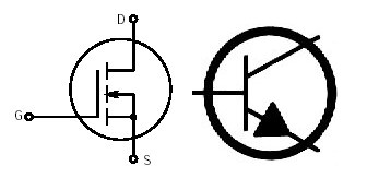
The limiting factor is the constancy of power gain over the entire power-output excursion. To visualise this, one can inspect the curve of output vs. drive power in the transistor data sheet. Generally, MOSFETs will exhibit superior linearity as compared to bipolar junction transistors (BJTs). MOSFETs such as the Motorola MRF150 began to displace BJTs (e.g. MRF448, 2SC2652) in the late 1990s. (Reference 5)
The higher the voltage excursion, the longer the linear portion of the output/drive power curve. For this reason, amplifiers powered from 40V or 50V DC exhibit considerably better linearity, and thus lower IMD, than 13.8V units. Typical 3rd-order IMD (IMD3) values relative to PEP are 32 dB for 50V and 24 dB for 13.8V. Additionally, the much higher current requirements of a 13.8V design (typically 100A peak for 500W PEP) render power-supply design much more difficult.
Extending this principle further, a tube amplifier, with its peak plate-voltage excursion of thousands vs. tens of volts, is more linear than any solid-state design (typically, IMD3 < -40 dB relative to PEP).
The collector-to-collector (or drain-to-drain) load impedance must be maintained as close to resistive as possible. This in turn requires optimising the wideband output transformer(s), combiner (if used), and low-pass filter passband VSWRs to as low values as possible. The load presented to the low-pass filter output must also be as close as possible to 50Ω resistive. Mistermination of the low-pass filter will degrade the filter's amplitude/frequency and phase/frequency response, and will also generate excessive RF voltages and/or currents which can cause serious damage. (Reference 1)
The exciter's IMD products will degrade the overall system IMD figure, as discussed here.
Efficiency: There is always a trade-off between amplifier efficiency (the ratio of RF output power to DC input power) and linearity. Solid-state amplifiers are generally operated Class AB (180º < conduction angle < 360º). This is a compromise between Class A (360º, most linear, least efficient) and Class B (180º, most efficient, least linear owing to crossover distortion). The devices are biased on to a standing current sufficient to minimise crossover distortion. It is possible to adjust the bias for minimum IMD3 by performing a 2-tone test at full rated PEP, and observing IMD3 on a spectrum analyser during the adjustment procedure.
As mentioned earlier, the efficiency of most solid-state HF amplifiers is approximately 45 ~ 50% at rated PEP. This compares favourably with many tube amplifiers, when one factors in the filament and screen power requirements of the latter.
Adequate power output: Solid-state amateur HF linear amplifiers generally fall into two power classes: 500W PEP and 1 kW PEP. All the current high-end offerings are 1 kW class.
The power output is limited by the maximum ratings of commonly available RF power transistors, and by the linear operating region of these devices. The most cost-effective designs employ multiple devices rated at 150W to 250W output each. As discussed in the Introduction, the devices are arranged in groups of two or four push-pull pairs, each module being capable of 250W output.
In the 1980s, popular 500W-class amplifiers used two pairs of BJT RF power transistors. The operating instructions recommended operation at 500W CW or PEP SSB output. Even though the 200W/device maximum rating offered some headroom, users were advised against exceeding 500W, as severe IMD3 degradation would result. In current 1kW-class MOSFET amplifiers, eight MOSFETs, each rated at 150W output, are arranged in four pairs. Headroom is somewhat less than for 200W BJTs, although IMD3 does not degrade quite as rapidly for Po > 1 kW. Typically, these amplifiers are comfortable at 1.0 to 1.1 kW PEP. MOSFETs have a higher cutoff frequency than BJTs, allowing full-power operation on 6 metres.
Power gain: This is the ratio of RF output to RF drive power. The system power gain of a given amplifier is the power gain of the PA devices minus the insertion loss of the input splitter, output combiner and output filters. The auto-tuner insertion loss must also be factored in, as applicable.
The power gain of any RF transistor decreases as frequency increases. This can be seen from the curve of power gain vs. frequency in the transistor data sheet. Typical values for system power gain at 14 MHz are 10 dB for BJTs and 12 dB for MOSFETs. This equates to drive power levels of 100W (BJT) and 65W (MOSFET) for 1 kW output. MOSFET power gain will typically increase by about 2 dB at 3.5 MHz, and decrease by 2 dB at 28 MHz (4 dB at 50 MHz). The frequency-dependent power gain roll-off of MOSFETs is somewhat less severe than that of BJTs.
The good news for radio amateurs considering a solid-state amplifier is that a 100W-class solid-state transceiver will drive it to full rated output.
Reduced-power operation: Some solid-state amplifiers feature a "Low Power" setting which reduces the drain (or collector) supply voltage to lower the maximum output by 3 dB. This is preferable to merely reducing the drive power by the same amount.
The problem is that the limiting condition for reduced-power operation is the onset of crossover distortion, which will degrade system linearity. Crossover distortion is significant at low drive levels. In Class AB operation, the bias is set to provide the best compromise between standing current and small-signal linearity; some crossover distortion is inevitable at settings which hold standing current (and its resulting dissipation) down to acceptable levels. It is thus best always to drive the amplifier to a point near the top of its linear operating region, where Edd(p-p) is just less than 2Vdd. This increases the margin on the device transfer characteristic between the peak voltage corresponding to PEP and the point where crossover distortion becomes significant. Lowering Vdd will achieve this objective, whilst lowering the power output by the desired amount.
QSK capability: Some earlier solid-state HF amplifier designs used open-frame input and output T/R relays. These relays were somewhat too slow-operating to follow full-break-in keying much in excess of 10 to 15 wpm.
Current designs utilise miniature high-speed sealed relays, which are rated for a life of many millions of operations. Carrier-on timing in the exciter prevents hot-switching by delaying the application of drive until the relays have switched. This will prolong relay life. In addition, some designs provide a transmit-inhibit line to a compatible exciter. This line enables the RF drive only when all relays in the amplifier's signal path have settled after keying.
Some amplifiers also offer a feature which exercises all relays in the amplifier, low-pass filters and auto-tuner by operating and releasing them periodically when the amplifier is idle, but powered-up.
Monitoring & Protection Features: The PA stage is fitted with sensors that measure a variety of operating parameters, and forward their readings to the system controller (microprocessor or logic board). These parameters include DC supply voltage and DC PA input current (total and per-module), RF drive power, RF power-device case temperature, per-module output power and total forward & reflected power (at the combiner output, the LPF output and the auto-tuner output). The controller also drives metering functions. At a minimum, these should include the following:
Reflectometers located between the PA combiner output and the LPF input, the LPF output and the auto-tuner input, and also at the auto-tuner output send forward- and reflected-power signals to the controller. These signals control auto-tuner settings; they also drive power-output and SWR metering and monitoring functions, and the ALC line. If the wrong LPF has been selected for the operating band, the reflectometer at the combiner output will detect high reflected power and signal the controller to shut down the amplifier. Likewise, if the load SWR exceeds the matching range of the auto-tuner (typically 3:1 max.) the reflectometer at the auto-tuner output reports high reflected power and signals the controller to lock the amplifier out. This feature protects the amplifier and auto-tuner against possible damage due to antenna-system failure.
At a minimum, the protection subsystem should detect the following anomalous conditions:
There are two stages of protective action; automatic drive fold-back via the ALC line, followed by amplifier shutdown or lockout. For example, drive fold-back may commence for SWR > 1.5:1, with 3dB reduction in output at SWR > 2:1* and lockout at SWR > 3:1.
Some amplifiers incorporate a simple, brute-force drive-limiting circuit in the RF input signal path. This serves to absorb initial RF power spikes generated by certain older exciters.
*In some designs, the controller signals the PSU to drop the collector/drain supply voltage to the "Low Power" value, thereby reducing output by 3dB for SWR > 2:1.
Automatic band selection is a feature of almost all solid-state amplifiers. This may be implemented in several ways; the exciter can supply coded band information to the amplifier via a proprietary protocol, or the amplifiers controller can count the excitation frequency and thus determine the correct band. The band-data input is one of the amplifier's external interfaces.
Once the controller has determined the operating band, it selects the correct
LPF for that band. In an amplifier with an internal auto-tuner, the
controller also presets the tuner to the setting last stored for that band.
(If the controller is aware of the drive frequency, it sets the tuner to the
previously-stored tuning point closest to that frequency.) ![]()
2. Controller & protective
circuits: Please refer to Monitoring &
Protection Features (above) for details. ![]()
3. ALC circuit:
Some form of ALC (automatic level control) should always be used to prevent driving the linear amplifier into the peak-flattening range - beyond its linear PEP capability. Excessive drive causes high IMD (splatter) on both sides of the signal. (Reference 1, Chapter 14.)
The ALC output feeds back a DC control voltage to gain-controlled IF stages in the exciter. This voltage is proportional to the amplifier power output. The ALC voltage is usually negative-going; the higher the voltage, the lower the exciter output (drive power). The purpose of the ALC is twofold:
(1) to limit the amplifier output to a preset level without causing distortion,
and (2) to reduce drive when the amplifiers protective subsystem detects an out-of-limits condition.
1: During normal amplifier operation, the controller derives the ALC voltage from the forward-power signal supplied by the reflectometer between the LPF output and the auto-tuner input. This is fundamentally different from the ALC derivation method used in most tube amplifiers, in which the ALC voltage is usually derived from PA-stage grid current. In a tube amplifier, the ALC prevents overdrive by reducing the RF drive at the onset of grid current.
As mentioned earlier, IMD degrades quite rapidly if the design power rating is exceeded (IMD3 rises by 3 dB, and IMD5 by 5 dB, for every 1 dB increase in Po over rated output.) To avoid this, the operator should adjust the ALC at the amplifier to hold the power output to the rated level. ALC should be adjusted in RTTY or CW mode, with the exciters RF output control set at 100%.
2: Upon detecting any of the anomalous conditions described above, the controller will also develop sufficient ALC voltage to reduce the drive to a safe level. (For example, the reflected-power signal generated by the abovementioned reflectometer reports a load mismatch to the controller, which in turn folds back the drive via the ALC line.)
Proper connection and adjustment of the ALC is absolutely mandatory when using a solid-state amplifier. The ALC line is the amplifiers first line of defence. Failure to properly configure ALC will place the costly RF power devices (and other components) at risk of destruction.
With the ALC correctly adjusted as per the amplifier manufacturer's
instructions, the exciter's drive power control should be set just
above the point where the amplifier delivers nominal power output,
rather than at maximum. This will minimise "ALC compression", and prevent
overdrive in the unlikely event of ALC failure. (Reference
4)![]()
4. Low-pass filter (LPF) box: This is the next component in the RF signal path. As mentioned above, the LPF box is a shielded enclosure containing a bank of bandswitched low-pass filters. These filters are usually Chebyshev networks, offering high attenuation and a steep roll-off near the cutoff frequency. They are designed to suppress harmonics and spurious emissions to levels required by radio regulations (typically 46 dBc or lower).
The filters are implemented using air-wound and ferrite-cored
inductors, and low-loss, high-Q, high-current capacitors (e.g. silver-mica). One
filter is provided per frequency band or range, and the filters are switched in
and out of the signal path via miniature high-speed sealed relays. Cooling air
is passed through the LPF box to remove heat caused by RF losses. The filter
insertion loss is typically 0.5 to 1 dB in the passband. ![]()
5. Auto-tuner: Some solid-state HF amplifiers are fitted with an internal auto-tuner. This is typically a T-network, with capacitive series arms and an inductive shunt arm. The capacitive elements are motor-driven air-variable capacitors, whilst the inductive element is a combination of air-wound and ferrite-cored coils, with relay-switched taps. A reflectometer at the tuner input (and, in some designs, a phase comparator measuring the phase angle between the tuner input and output) signal an optimum match condition to the controller when reflected power is minimal and the input/output phase shift is exactly 180º. This stops the capacitor drive motors.
Another approach utilises a reflectometer and a return-loss bridge at the auto-tuner input. The controller initially reads the reflectometer for coarse tuning, then switches the return-loss bridge into the tuner-input signal path for fine tuning. The capacitor drive motors are stopped at the point of maximum return loss.
In some amplifier designs, the controller either bypasses the PA stage, or inserts a 20 db attenuator in the PA-output signal path, to minimise interference to other stations during the tuning cycle.
Typically, the auto-tuner is designed to match load impedances in the range 16-150Ω resistive (load VSWR = 3:1 max.) Insertion loss is 0.5 dB when matched to VSWR < 1.5:1 at the tuner input. The auto-tuner is not intended to match highly reactive loads, such as non-resonant antennas; a suitable external tuner can be connected to the amplifier output for this purpose.
The auto-tuner must be disengaged when using an external tuner. Cascading tuners can reflect high reactance values back into the auto-tuner and/or LPF. As a result, dangerously high RF voltages can appear across capacitors in these networks, leading to component failure.
An internal auto-tuner in a 1kW-class amplifier requires some cooling, to remove heat generated by losses in the inductors and fixed capacitors. This is accomplished by a small fan in the auto-tuner compartment, or by the diversion of a portion of the amplifier cooling air through the tuner area. (For 1 kW delivered to the load, with 0.5 dB insertion loss, the auto-tuner T-network dissipates 125W).
Depending on the controller design, the auto-tuner may either track frequency
and load-impedance changes dynamically, or store and hold settings previously
established during a tuning cycle. The controller also switches taps on the
inductor, and switches in fixed capacitors as needed for the lower frequency
ranges. ![]()
6. External interfaces: In addition to the usual RF input, RF output (antenna), keying, ALC and power connectors, a solid-state amplifier is usually fitted with a "Band Data" input. This enables the exciter to send band-selection information to the amplifier controller. The band-data format is proprietary, and unique to each equipment manufacturer. In some designs, a reverse-keying line allows the amplifier to key the exciter, to request a carrier. The amplifier controller counts the carrier frequency to set the correct frequency range. This feature preserves automatic bandswitching when the amplifier and exciter are of different makes.
Many solid-state amplifiers offer dual RF input, keying and ALC interfaces, allowing the operator to switch between two exciters. Separate ALC adjustments are provided for the two inputs. In addition, up to four selectable RF outputs may be provided. These may be programmable, to permit automatic antenna selection by frequency range or band.
The keying (PTT) line in a solid-state amplifier is low-level, and is designed to be driven by an open collector or a light-duty reed relay in the exciter. No auxiliary keying relay or buffer is required. Some designs support QSK with a compatible exciter, via the keying line and a transmit-inhibit line.
Depending on equipment configuration, the external interfaces (other than
power and RF) may be grouped in multi-pin connectors, to facilitate
interconnection with the exciter. In addition, keying and ALC lines are usually
brought out to RCA jacks.![]()
7. Power supply unit (PSU): The PSU may be internal or external; both linear and switching types are encountered. Generally, 500W-class amplifiers are sold with a companion 1.5 kVA linear PSU rated at 40V 25A output, whereas a 2.5 kVA switcher rated at 48V 50A output is provided with a 1kW-class amplifier. The PSU incorporates inrush-current limiting. Some 48V PSU designs allow switching to a lower output voltage (typically 35V) for half-power operation of the associated amplifier.
A well-designed PSU will incorporate extensive RF decoupling.
To ensure optimum linearity, the PSU must be well-regulated (approximately 5% output voltage drop at full load). A well-regulated collector/drain DC supply is essential to obtaining good linearity. It allows optimising the collector-to-collector (or drain-to-drain) load resistance for good efficiency and controlled current swing, without going into saturation.
The base- or gate-bias regulator must be absolutely stable and free from RF or envelope modulation. Careful attention to the bias supply performance is necessary for the best linearity of which the power devices are capable. To reduce standing collector (or drain) dissipation in the RF power devices, bias voltage is applied only when the PTT line is in the transmit state. During standby, the devices are at zero-bias (non-conducting). RF-sensing electronic bias switching is not normally used in a solid-state amplifier.
Operation from 220 ~ 240V mains is recommended, to minimise the effects of mains-voltage drop. The PSU should incorporate an adequate forced-air cooling system. A two-pole circuit breaker in the primary mains circuit is an excellent safety refinement.
A remote-control panel is a convenient operating feature
offered with some high-end solid-state amplifiers. ![]()
The above article is also available in Russian. ![]()
Read Matt, KK5DR's article "What makes a good tube-type HF amplifier?"
Also by Matt, KK5DR: "Building a tube-type HF
amplifier" (in Russian) ![]()
View typical examples of commercially-available solid-state amateur HF/6m amplifiers.
References:
Acknowledgements:
Copyright © 2002 A. Farson VA7OJ/AB4OJ. All rights reserved. Last updated 06/09/05