LAST MODIFIED:
Wednesday, 30-Jun-2004 19:36:48 PDT
What exactly is a buffer amplifier, what is its purpose in life?
This class of amplifier is designed to follow low level stages, one example is a crystal oscillator. An oscillator for optimum performance can NOT be loaded down, it needs an intermediate stage following. This will then present a sufficiently high enough input impedance so it is not considered a significant load to the oscillator. The intermediate or buffer stage, while not representing a load must then have a sufficiently low output impedance to drive successive stages.
If these concepts of impedance confuse or worry you then look at my other page "what is impedance?" it's a rough and ready explanation, followed by a more technical explanation of impedance matching but hopefully you will come back with a considerably better understanding.
From what I said above, two desirable traits of a buffer amplifier are high input impedance and low output impedance. Obviously succeeding stages should also be linear because we don't want to introduce distortion.
As a matter of interest a buffer amplifier is not solely limited to following an oscillator. You could have a requirement of wanting to sample the output of the first mixer for what is called a "Panadaptor", a means of visually seeing adjacent signals on an oscilloscope. Also a high quality agc system should be derived from the last i.f. stage, it should be buffered before going to the agc amplifier and then on to the agc detector.
Other examples are low level outputs of audio amplifier stages such as microphone inputs where the microphone is a high impedance type. Although not so common now, phono inputs to audio ampliers also needed buffering.
Here I'm going to use a very practical example where one of my readers has a requirement for a voltage controlled oscillator operating at 1.8 - 2.0 Mhz (amateur radio band 160M). This is to be part of a frequency synthesiser.
The design requirements were:-
(a) frequency coverage 1.8 - 2.0 Mhz
(b) voltage controlled by a frequency synthesiser with an output level sufficient to drive the input of a Phase Locked Loop (PLL)
(c) a further buffered output for a digital frequency readout.
(d) another buffered out put to drive succeeding amplifier stages.
We can look at two types of active devices for use in buffer amplifiers, FET transistors and bipolar transistors. Choice is largely a matter of opinion but more often it depends on what you have on hand. Bipolar types are referred to as "emitter followers".
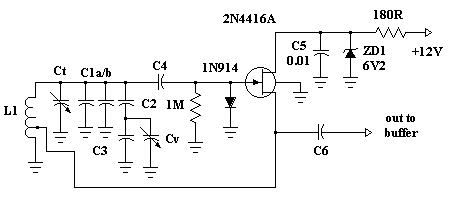
Let's look again at our previous oscillator.

Figure 1 - schematic circuit of a hartley oscillator
Now it is considered bad practice to use the output of the oscillator to
drive succeeding stages because in loading down the oscillator we cause
frequency pulling and a host of other unwanted maladies.

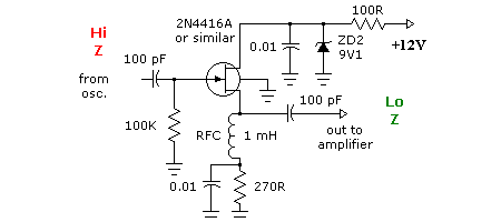
Figure 2 - schematic circuit of a FET buffer amplifier
That's about as basic as it gets. The FET represents a high input impedance (Z) but a relatively low output impedance. This buffer amplifier configuration, called a "source follower", is capable of high power gain, perhaps as much as 25 db BUT the voltage output would be only around 90% of the input which is a voltage gain of -0.5 dB (loss)
Confused?. Look at it this way - consider an input signal of say 50 mV RMS. I've just said the output voltage is about 90% or in this case 45 mV, yet I spoke of Power Gain, in fact 25 dB perhaps. Assume for purposes of discussion only, that the input impedance is 100K or 100,000 ohms.
It follows that input power taken from the preceding stage is P = E2 / R or [ ( 0.05V * 0.05V ) / 100,000 which equals 0.025 micro-watts.
If the output power available to the succeeding stage is assumed to be sourced from a relatively low 270 ohms source, albeit at a reduced voltage of 45 mV RMS, then our calculations are P = E2 / R or [ ( 0.045V * 0.045V ) / 270 this equals 7.5 micro-watts.
It further follows that for 7.5 uW output after a 0.025 uW input there must have been a power gain of 7.5 / 0.025 = 300 which 10 * log (300) = 24.77 or say 25 dB.
I am not saying this is the case. I am merely highlighting the capability and the basic underlying principles.
If you are involved in electronics then consider joining our "electronics Questions and Answers" news group to ask your question there as well as sharing your thorny questions and answers. Help out your colleagues!.
The absolute fastest way to get your question answered and yes, I DO read most posts.
This is a mutual help group with a very professional air about it. I've learn't things. Not for absolute newcomers to ask questions BUT it is an excellent learning resource for lurkers.
broad band amplifiers
emitter degeneration
negative feedback
small signal amplifiers
NEW! - How to link directly to
this page
Want to create a page link to me from your site? It couldn't be easier. No HTML knowledge required; even the technophobes can do it. All you need to do is copy and paste, the following code. All links are greatly appreciated; I sincerely thank you for your support.
Copy and paste the following code for a text link:
and it should appear like this: <a
href="http://www.electronics-tutorials.com/amplifiers/buffer-amplifiers.htm"
target="_top">visit Ian Purdie VK2TIP's Buffer Amplifier
Page</a>
visit Ian Purdie VK2TIP's Buffer Amplifier Page
|
Looking for more? Visit my site map page:

This site is hosted at WebWizards.Net for better value.
Tell your friends, tell a news group, tell your favourite magazine, heck tell the world!
the author Ian C. Purdie, VK2TIP of
www.electronics-tutorials.com asserts the moral right to be identified as the
author of this web site and all contents herein. Copyright © 2000, all rights
reserved. See copying and
links. These electronic tutorials are provided for individual private use
and the author assumes no liability whatsoever for the application, use, misuse,
of any of these projects or electronics tutorials that may result in the direct
or indirect damage or loss that comes from these projects or tutorials. All
materials are provided for free private and public use.
Commercial use
prohibited without prior written permission from www.electronics-tutorials.com.
Copyright © 2000, all rights reserved. URL - http://www.electronics-tutorials.com/amplifiers/buffer-amplifiers.htm
Updated 15th May, 2000