An 80 Meter CW Five Watt QRP Transceiver
by Anthony “Goody” Good K3NG
Please excuse the dust – this is under construction like most of the Internet.
Updated 2003-09-21
Introduction
This project originally started out on the bench as a 40 meter phone transceiver. I was intending to build a phasing type SSB modulator, but lost interest after I ran into a brick wall with the design. Wanting to build a QRP with different capabilities than my other QRP rigs, I decided to go to 80 meters. In one evening I changed various parts to transform the project into an 80 meter rig.
Several parts of the circuits came from various classic QRP texts. I have changed the circuits in various areas for better performance, at least with my construction of it, or made changes based on the components I had on hand. Other changes are just variations that I made on a whim to see what would happen. Where the circuit largely remains like the original one, I have given credit to the original author.
I don't claim to be a professional designer. My QRP building and design philosophy is if it works, doesn't cost too much, and doesn't catch fire, it's probably a decent workable design. I'm sure other more seasoned engineers could improve this design. I welcome any constructive feedback.
Each circuit description includes a table describing the “plain English” function of each component to assist beginners in learning and serve as an exercise for myself. I was always disappointed with sparse circuit descriptions while learning as a teenager.
This project is an intermediate level project. You should have a couple small kits under your belt and perhaps some Manhattan construction experience as well. I'd recommend having a frequency counter and oscilloscope available. You may (will !) need to tweak parts of this circuit as I have built only one prototype. In other words, your mileage may vary. But don't let me discourage you. Just get the iron out and start building !
|
|
|
|
|
|
|---|
Block Diagram Level Description
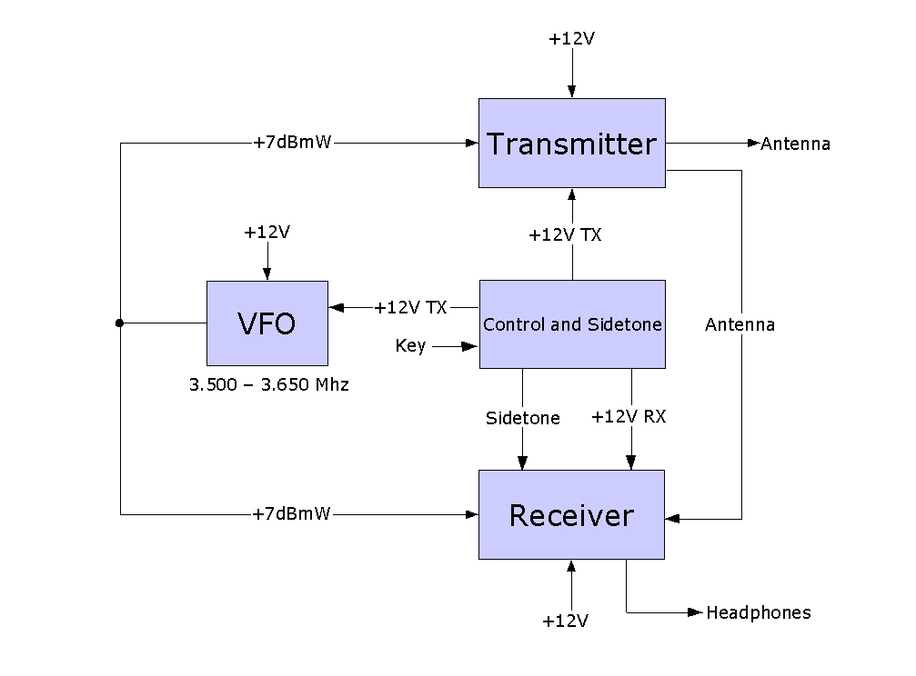
The Control and Sidetone module distributes supply voltages during transmit and receive to the appropriate sections. It also creates the sidetone that is fed to the receiver audio section during transmit.
The rig uses a Variable Frequency Oscillator directly on the operating frequency. The VFO output is fed to the transmitter and receiver sections, with level of about +7dBmW. The VFO is on continuously. On transmit, the VFO frequency is “pulled” down about 700 hertz to provide the necessary transmit frequency offset.
The receiver is a direct conversion type. It mixes the VFO signal with the incoming signal from the antenna to produce a CW beat note that is amplified and output to the headphones. The receiver is muted during transmit.
The transmitter amplifies the VFO signal and outputs 5 watts of power to the antenna. The transmitter also contains diodes for QSK T/R switching and connects the receiver to the antenna during receive.
VFO Circuit Description
Schematic – high resolution BMP format (3.9M)
The VFO is a classic Colpitts design with two buffer stages and a varicap diode used for tuning. Minimal coupling between the oscillator (Q100) and the first buffer (Q101), 20 pF , is used to minimize pulling of the oscillator frequency. I chose an inductor-tap feedback as opposed to a capacitor-divider feedback to minimize the parts counts, as I'm always leery about adding more capacitors which ultimately make the circuit less stable. I've found the inductor-tap design produces a less linear waveform than the capacitor-divider feedback method, but the low pass filter before the output of the VFO cleans things up, so it doesn't really matter.
The output of the VFO is split into to 50 ohm outputs to feed the receiver and transmitter sections with about +7 dBmW of power. To increase the output level of the VFO, increase the value of the interstage coupling capacitors C108 and C109.
After warm up, the VFO is pretty stable only moving a couple hertz plus or minus.
|
Designation |
Value / Device |
Type |
Function |
|---|---|---|---|
|
R101 |
10K |
10 Turn |
Tuning voltage for varicap diode D100. Main VFO Tuning on front panel. |
|
R102 |
2.2K |
¼ W |
This raises the lower end of R101 about 1 volt and determines the lowest tunable frequency. This was put in to limit the bandspread of R101 and account for the non-linearity of D100 at the lower end of the voltage curve. |
|
R100 |
47K |
¼ W |
Isolates the RF at C100 and D100 from the tuning pot, R101. |
|
C103 |
0.001 |
disc ceramic |
Makes an “RF ground” on the one end of R100, so RF doesn't “see” the long leads to R101 and shunts any RF garbage picked up from R101's leads to ground. |
|
D100 |
MV2115 |
varicap diode |
This changes capacitance with the voltage determined by R101. Higher voltage, less capacitance, higher oscillator frequency. Other varicaps could be used if the value of C100 and L100 is tweaked. |
|
C100 |
680pF |
polystyrene or NP0 disc ceramic |
Blocks tuning voltage on D100 from the rest of the circuit and forms a tuned circuit with D100, C101, L100, and C106 to determine the oscillator frequency. |
|
C101 |
220pF |
polystyrene or NP0 disc ceramic |
Part of the oscillator tuned circuit (see C100). |
|
L100 |
34 turns on T60-S iron powder core, tap at 11 turns up from ground |
toroid |
Part of oscillator tuned circuit. Tap point determines how much feedback is fed from Q100's source. Tap also provides a DC ground point for Q100's source. The tuning range of the oscillator can be adjusted by spreading or crunching L100's turns. L100 should be coated with Q-Dope to minimize drift and microphonics (noise from physical circuit board vibrations). I constructed the rig with L100 vertical rather than on its side. |
|
C102 |
20pF |
NP0 ceramic disc |
Blocks Dc voltage at R104, D101, and Q100's gate and slightly affects the oscillator frequency. |
|
R104 |
100K |
¼ W |
Sets up bias for Q100. |
|
D101 |
1N914 or 1N4149 |
|
Sets up bias for Q100 and clamps negative voltage swings and stabilizes oscillator. |
|
Q100 |
MPF102 |
FET |
Active device for the oscillator stage. |
|
D102 |
6V |
Zener diode |
Regulates the voltage on Q100's drain at six volts. This is so the circuit is more stable. Typically lower voltage oscillators are more stable. This is also a good technique to keep garbage on the VCC line from affecting the VFO frequency. This voltage could be increased with another zener diode to produce more output power at the expense of stability. |
|
R103 |
270 ohms |
¼ W |
Current limiter for D102, forms a resistor divider with D102. Also isolates noise from the DC line. |
|
C104 |
.01uF |
disc ceramic |
Bypasses any RF coming from the VCC line to ground and keeps D102 from acting like a RF detector and picking up garbage. Also looks like an RF ground to Q100. |
|
C106 |
10pF |
trimmer |
This capacitor is “turned on” by D1 and D2 on transmit to pull the frequency down about 700 Hz to provide the necessary TX offset. The capacitor also slightly affects the oscillator when not turned on. |
|
D103 |
1N914 or 1N4149 |
diode, general purpose |
Conducts when the voltage comes through R105 to ground through L101 (as does D104), thus making C106 look like it has a ground and pulls the oscillator frequency down as the oscillator circuit has more capacitance. |
|
D104 |
1N914 or 1N4149 |
diode, general purpose |
See D104 |
|
L101 |
100uH |
molded inductor |
Provides a ground path for voltage flowing through D103 and looks like a high impedance to RF, so C106 is unaffected by the ground connection needed for DC. |
|
R105 |
2.2K |
¼ W |
Limits the current flowing through D103 and D104 and isolates the TX DC line from the circuit. |
|
R106 |
1K |
¼ W |
Put in for good measure. I noticed when testing with alligator clips, the offset circuit was affecting the oscillator when the one end of R105 was left floating. This resistor just “pulls” it to ground and insures there is no noise being picked up and affecting the circuit. This may be possibly omitted. |
|
IC100 |
7812 |
voltage regulator |
Put in for good measure. This regulates the DC line into the VFO at 12 volts, minimize voltage changes and contributing to stability, especially when battery operated. Also isolates the VFO from the rest of the rig and keeps garbage on the DC line from other stages from getting into the VFO. Could be omitted, but the extra fifty cents is worth it. |
|
C105 |
10uF |
electrolytic at least 15 working volts DC |
Voltage regulation on the DC line. |
|
C108 |
20 pF |
disc ceramic |
Couples the signal from Q100 to the next stage; isolates the DC bias on the gate of Q101 from the DC ground on the source of Q100. Increase the value of this capacitor to increase the output level of the VFO, at the expense of some frequency stability. |
|
R107 |
100K |
¼ W |
Sets up bias on gate of Q101 |
|
Q101 |
MPF102 |
FET |
Active device of this stage, a buffer amplifier |
|
L102 |
100uH |
molded choke |
Looks like 0 ohms to DC, and a 2K reactance to the operating frequency. This sets up the output impedance for the amplifier |
|
R109 |
100 ohms |
¼ W |
This limits the DC current through Q101. |
|
C114 |
.01uF |
disc ceramic |
Provides an RF ground for L102, so RF doesn't “see” R109. |
|
R108 |
100 ohms |
¼ W |
Isolates this stage from the DC line so supply variations will have less of an effect. |
|
C110 |
.01uF |
disc ceramic |
Creates an “RF ground” on the drain of Q101 and also shunts any RF garbage coming down the power supply line |
|
C109 |
82pF |
disc ceramic |
Couple the signal from the Q101 buffer amplifier to the Q102 buffer stage. Isolates DC bias voltages between the two stages. Increase the value of this capacitor to increase the output level of the VFO. |
|
R111 |
15K |
¼ W |
Forms a voltage divider with R112 to place about 3.3 volts on the base of Q102. |
|
R112 |
5.6K |
¼ W |
See R111 |
|
R113 |
330 ohms |
¼ W |
Emitter resistor on Q102. Limits the amount of current through Q102, and sets up the resting operating point for Q102. The base voltage is about 3.3 volts, so the emitter voltage would be 2.6 volts, making an emitter current of 7.8 mA. Having an emitter resistor stabilizes the amplifier, as the resting current will be determined by the emitter resistor and not the beta of transistor, which can vary from device to device. |
|
C116 |
.01uF |
disc ceramic |
An “RF bypass” for R113. This increases the gain of the stage at RF frequencies without increasing the resting DC current. |
|
Q102 |
2N2222 |
bipolar NPN general purpose transistor |
Active device of the stage. |
|
L104 |
9.9uH |
45 turns of #26 wire on a T50-2 core, or a molded choke |
Looks like 220 ohms reactance at the operating frequency, but 0 ohms at DC. RF current swings create the voltage swing that is the output of this buffer. |
|
R110 |
270 ohms |
¼ W |
Isolates the DC supply line from the stage. Could possibly decrease the value of this to increase the output power of this stage. |
|
C115 |
0.01 |
disc ceramic |
Provides an RF ground on the other side of L104 so that RF doesn't flow back into the DC supply line, and the RF on the collector of Q102 “sees” a consist reactance. Also shorts RF garbage coming down the DC line. |
|
C117 |
0.01 |
disc ceramic |
Isolates the DC voltage on the collector of Q102 from the low pass filter and subsequent stages. |
|
C118 |
820pF |
disc ceramic |
Forms a low pass filter along with L105 and C119. The low pass filter filters out any harmonic energy which would be later amplified by the transmitter stage, or cause spurious responses (or images) in the receiver. The reactance of C118 and C119 decrease with frequency, while the reactance of L105 increases with frequency. Thus, the higher you go in frequency, the more attenuated the signal becomes, thus forming a low pass filter. C118, L105, and C119 each have a reactance of about 50 ohms at the operating frequency. |
|
L105 |
2.2 uH |
21 turns #28 enameled wire on a T50-2 iron powder core |
See C118 |
|
C119 |
820pF |
disc ceramic |
See C118 |
|
R114 |
50 ohms |
¼ W |
Forms an “RF splitter” with R115 to split the output of the VFO. This presents a 50 ohm impedance to the low pass filter, the receiver module, and the transmitter module. |
|
R115 |
50 ohms |
¼ W |
See R115 |
|
C120 |
220pF |
disc ceramic |
Has a reactance of about 200 ohms at the operating frequency and is used to sample some of the signal for a high impedance input frequency counter to aid in tuning. Decrease the value so that you have just enough signal to trigger the frequency counter. |
Receiver Circuit Description
Schematic - High Resolution BMP format (5.6M)
The receiver is a direct conversion type. The first stage is an preamplifier based around Q400 with a primitive, yet effective means of controlling RF Gain through the use of emitter degeneration via R403. The signal is then feed into a diode mixing consisting of D400 through D 403. The local oscillator signal (LO) from the VFO is fed into the mixer which is mixed with the incoming signal from the antenna, producing a beat that is our signal of interest. The remaining stages are audio amplifiers. Q401 forms a basic class A amplifier. Q402, Q403, and Q404 are all low pass amplifiers that provide some selectivity, attenuating audio signals above about 2 kHz. Q405, Q406, and Q407 provide the final amplification to drive a pair of headphones.
The preamplifier originally came from a Doug Demaw design. Stages based around Q401 through Q405 came from Sold State Design for the Radio Amateur, Page 82, Figure 24, which I believe was originally a W7ZOI design.
|
Designation |
Value / Device |
Type |
Function |
|---|---|---|---|
|
T400 |
|
toroid |
This forms a frontend filter and presents the proper impedance to the first stage amplifier. The primary couples the antenna signal to the secondary which is a tuned circuit formed by the secondary and C400 and C401. |
|
C400 |
120pF |
disc ceramic |
Part of the frontend filter |
|
C401 |
40pF |
trimmer |
Part of the frontend filter, tuned for maximum receive signal in the middle of the band |
|
C403 |
0.1 |
disc ceramic |
Couple the signal from T400 to the Q400 amplifier stages and blocks the Q400 base voltage from the ground of T400's secondary. |
|
R400 |
56k |
¼ W |
Forms a voltage divider with R401 to provide the base voltage biasing for Q400. |
|
R401 |
10k |
¼ W |
See R400. |
|
C402 |
0.1 |
disc ceramic |
Bypasses garbage on DC line to ground and makes the one side of R400 “look like” an RF ground (thus R400 is part of the input impedance at RF frequencies). |
|
R402 |
100 |
¼ W |
Limits the Q400 collector current. |
|
T401 |
|
toroid |
Forms a tuned circuit with C405 and C406 and couples the signal to the next stage. |
|
R405 |
470 |
¼ W |
Dampens the Q of the T401/C405/C406 tuned circuit and prevents oscillations from occurring. |
|
C405 |
120pF |
disc ceramic |
Forms the output tuned circuit with T401 and C406. |
|
C406 |
40pF |
trimmer |
See C405. Tuned for maximum receive signal in the middle of the band. |
|
Q400 |
2N2222 |
NPN transistor |
Active device for the preamplifier stage. Operated class A. |
Transmitter Circuit Description
Schematic - High Resolution BMP format (2.1M)
The transmitter section amplifies the signal from the VFO to a level of five watts, sending the signal out the antenna. Stages based around Q300 and Q301 are keyed during transmit. Q300 is a class A tuned amplifier, while Q301 is a tuned class C amplifier. Q302, the final PA transistor, is a class C amplifier that is continually powered with 12 volts. A low pass filter consisting of C312, C313, C314, L301, and L302 filters out all the harmonic garbage generated from the class C stages to provide a clean signal on the desired frequency. T/R switching of the receive antenna is provided by D301 and D302 which conduct on transmit, shorting one end of C312 to ground.
|
Designation |
Value / Device |
Type |
Function |
|---|---|---|---|
|
|
|
|
(under construction) |
|
|
|
|
|
T/R Control Circuit and Sidetone Circuit
Schematic – High Resolution BMP format (1.48M)
The T/R circuit provides the appropriate TX and RX voltages, which turn on the TX offset and the first two stages of the transmitter section, while turning off the first amplifier in the receive section. It also supplies voltage to the sidetone circuit and mutes the receiver section mixer/detector by providing voltage to Q408.
The sidetone circuit produces a sweet perfect sine wave ( I hate raspy modified square wave side tones that some rigs produce ! ). The frequency is determined by R207 and R208, the higher the value, the lower the frequency. The values shown produce 600 Hz almost exactly with my circuit. Replace one of these with a trimmer pot to vary the sidetone frequency.
|
Designation |
Value / Device |
Type |
Function |
|---|---|---|---|
|
|
|
|
(under construction) |
|
|
|
|
|
Construction
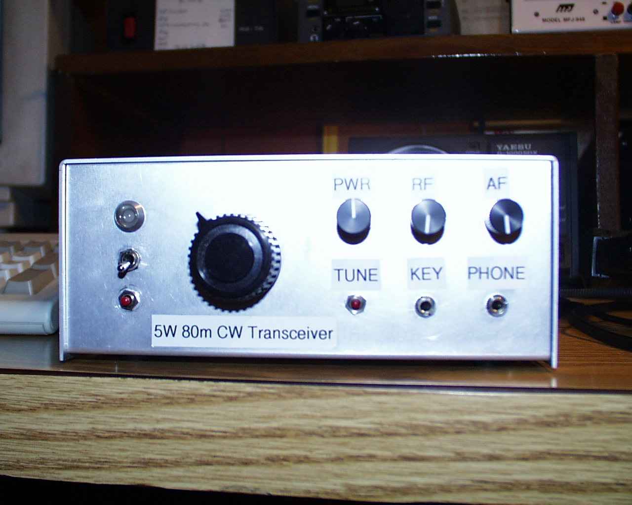
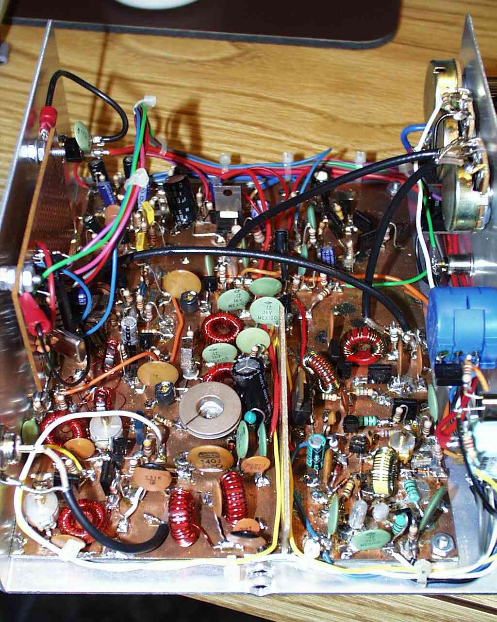
I enclosed this rig in a Ten Tec TP-47 unfinished aluminum enclosure ( 3” x 7.25” x 6” / H x W x D ). The circuit was constructed Manhattan style on a copper clad board about 5” by 6.25”.
Tuning
Receiver: C400 and C406 should be tuned for maximum receive signal in the middle of the band or primary area of operation such as the 80 meter QRP frequency, 3.560 MHz.
Transmitter: C303 and C307 should be tuned for maximum transmit power. Back off R300 if the output power exceeds five watts. You can also increase the value of R304 if the transmitter output runs hot. If using an antenna tuner, drop the power down to a watt or so to help extend the life of Q302. ( I didn't have any problems blowing the final PA after I installed D300 ).
VFO: Spread or compress the turns on L100 to adjust the VFO frequency range. I adjusted it so the bottom of R101 is 3.500 Mhz or so, the bottom of the band. Adjust to your person preference. The range of tuning can be adjusted by either placing resistors on either side of R101 to reduce the voltage swing going to D100, or by adjusting the value of C100. Increasing the value of C100 will increase the range, decreasing will lower it. Changing the value of C100 will also shift the center frequency of the VFO, which can be corrected by adjusting L100 as described above. C106 adjusts the amount of the negative transmit frequency offset. Adjust this so the rig transmits about 600 hertz (or whatever your favorite receive beat note frequency is) below the receive frequency with a frequency counter connected to the sample port at C120.
Sidetone and Control: Adjust R209 to your liking for the sidetone level. R207/R208 can be adjusted for your favorite sidetone frequency. C201 and R201 can be changed to soften the waveform of the transmitted CW if key clicks or harshness is observed.
Operation
As this rig has a direct conversion receiver, signals can be heard on both sides of zero beat. In other words, when tuning up the band, you will hear a signal with a high frequency beat note, decreasing as you tune up. The beat frequency continues to get lower until reaching zero beat (dead on the transmit frequency of the other station). Tune further up, and the beat reappears as a low frequency and increases frequency as you continue to tune upwards. This characteristic of direct conversion receivers require a little more thought when tuning on stations and attempting a QSO. Since the transmitter frequency is negatively offset (TX frequency is 600-700 Hz below the RX frequency), one needs to tune on the “high side” of zero beat in order to have the transmit frequency fall within the other station's receiver pass band.
Possible Design Improvements
CW Filter
A tight CW filter could be added between the Q405 stage and Q406 in the receiver audio sections. I find the 80 meter CW band isn't that congested, so it's not too much of a problem.
Audio Gain
I'd like a little more audio gain. Perhaps a CW filter with some gain would provide a little more audio power. On my rig I have to crank the audio gain all the way up.
RIT
Switch R102 with a variable resistor during receive activated a switch on the front panel. This would adjust the tuning voltage creating a RIT control.
Front End Amp
I've noticed the first receive amp can break into oscillations. Adjusting the RF gain will change the frequency or cause it to cease.
TX Power and RX Gain Controls
These aren't too linear. Someday I'll improve this.
Acknowledgments
Many thanks to Doug Demaw W1FB, SK, and Wes Hayward W7ZOI for their designs and outstanding contributions to QRP and Amateur Radio in general. Without them, I doubt I would have gotten interested in QRP or circuit building.
See you on 80 ! :-)